Piezoelectric MEMS
PiezoMEMS
Our piezoelectric MEMS are based on high-quality PZT film deposition technology and piezoelectric thin film formation and processing.
The PZT film (lead zirconate titanate thin film), which has a proven track record of mass production at our group company, offers both an excellent figure of merit (FOM) and high reliability.
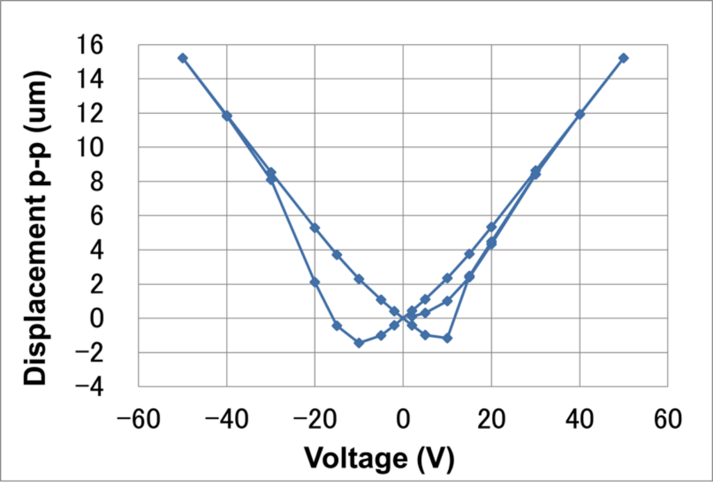
It achieves the stable electrical-mechanical conversion performance required for MEMS transducers.
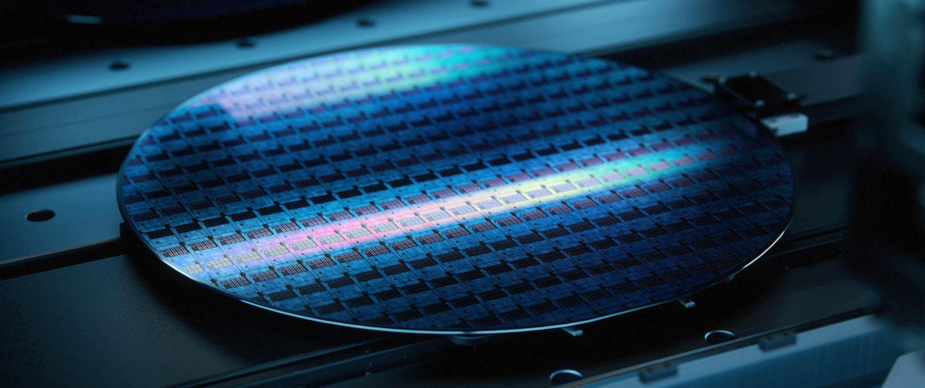
Furthermore, as part of our MEMS foundry services, we expanded our 8-inch (200mm) line for piezoelectric MEMS in 2020.
We have established a system that allows us to gradually expand our scale from research and development applications to mass production phases.
We can handle everything from piezoelectric thin film formation to MEMS device fabrication, providing a complete, integrated process.
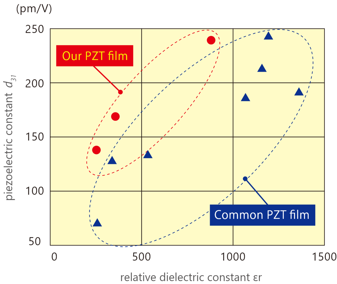
We offer a lineup of multiple PZT piezoelectric films, each with characteristics suited to different applications.
Built on PZT films with proven mass production at our group, we can optimize PZT deposition conditions and film structure to meet the needs of various piezoelectric MEMS applications.
From thin-film deposition to device fabrication, we offer flexible process design and development tailored to MEMS transducer requirements.

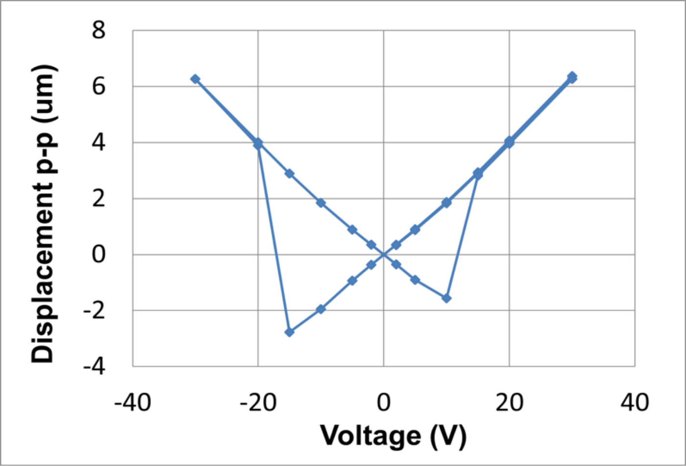
PZT piezoelectric thin films with a high piezoelectric constant d 31 are suitable for MEMS actuator applications that require the efficient generation of large drive displacements.

PZT films, characterized by their low dielectric constant εr, are suitable for MEMS sensor applications where high-sensitivity detection is required while suppressing noise.

The balanced PZT piezoelectric thin film, possessing both low εr and high d31, has characteristics suitable for MEMS transducer applications where both sensor and actuator functions are required.
MEMS actuator applications
High piezoelectric constant d31(PZT-O*))
MEMS sensor applications
Low dielectric constant εr(PZT-A*))
MEMS transducer applications
Balanced type with both low εrand high d31(PZT-B*))
*) PZT-O is a Poly film, and PZT-A and PZT-B are both Epi films, but A and B have different composition ratios.
| PZT-O | PZT-A・PZT-B | |
| Piezoelectric constant d31(pm/V) | 210 ~ 240 | 150 ~ 200 |
|---|---|---|
| Relative permittivityεr | ~ 900 | 260 ~ 500 |
| Film thickness(μm) | 1 ~ 5 | 2 ( standard ) |
| Others | Low stress +30MPa | High FOM*) > 50GPa |
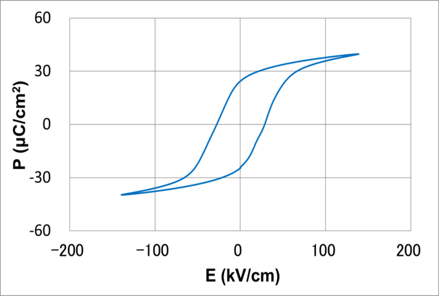
Polycrystalline PZT films, which exhibit high piezoelectric constants, have been used in a wide variety of applications, primarily in piezoelectric MEMS actuators.
We provide stable performance in piezoelectric MEMS devices where reliability is paramount.
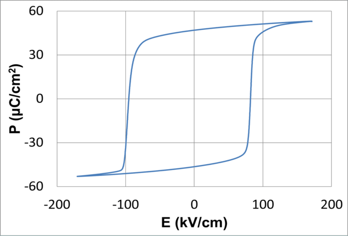
Based on previous experience, the newly developed PZT epitaxial film significantly reduces the dielectric constant while suppressing the decrease in the piezoelectric constant.
This results in a piezoelectric thin film that is ideal for MEMS transducers and sensors that require high sensitivity, low noise, and high FOM.
Using Predeus, manufactured by SPP Technologies Co., Ltd., a Sumitomo Precision Products group company with a proven track record in mass production of MEMS devices, we optimize verticality, sidewall roughness, and CD loss.
We offer world-class high selectivity and high etch rates, enabling us to perform highly challenging machining operations.
What is KNN piezoelectric thin film?
KNN piezoelectric thin films are environmentally friendly, lead-free piezoelectric materials that enable next-generation lead-free MEMS devices.
Amidst stricter environmental regulations such as the RoHS Directive and growing interest in ESG management, there is a need for lead-free MEMS as an alternative to conventional PZT (lead zirconate titanate).
It achieves both reduced environmental impact unique to lead-free materials and high device performance. By using it interchangeably with PZT film depending on the application,
We address the diverse development needs of next-generation MEMS transducers.
KNN membrane processed cross section
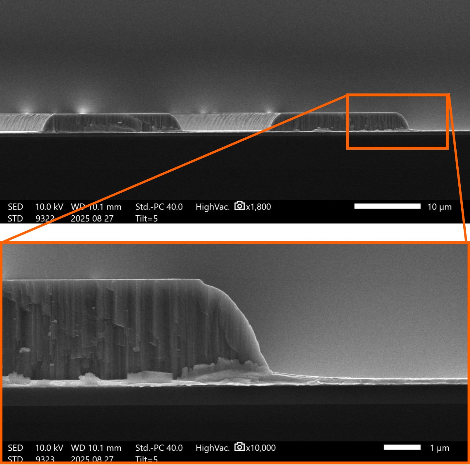
Tapered etching to improve upper electrode coverage
Among lead-free piezoelectric thin films, KNN is attracting particular attention as a material with great potential for practical application in MEMS devices.
Because it does not contain lead, it not only complies with environmental regulations but can also be used in applications where lead use is restricted, such as in the medical and biotechnology fields.
While film deposition and processing require sophisticated process control, this technology is expected to have applications in environmentally friendly MEMS transducers and new piezoelectric MEMS devices.