Si DRIE Technology
Deep Si etching
Our company is a joint development partner of the 'Bosch process,' which is essential for modern MEMS manufacturing, and a pioneer in Si processing.
Since releasing the world's first practical device in 1995, we have leveraged the knowledge we have accumulated over many years to provide unparalleled technical capabilities in high-precision, highly complex silicon deep etching.
Si Deep Etching (Si DRIE) is an essential foundational technology in MEMS silicon processing. Leveraging our long-cultivated equipment technology and process know-how, we provide comprehensive support for MEMS devices using Si Deep Etching, from design and prototyping to evaluation and mass production preparation.
Deep Reactive Ion Etching (DRIE) is a silicon etching technique used in MEMS silicon processing.
By processing silicon substrates deeply with high anisotropy, it becomes possible to form fine and high aspect ratio structures.
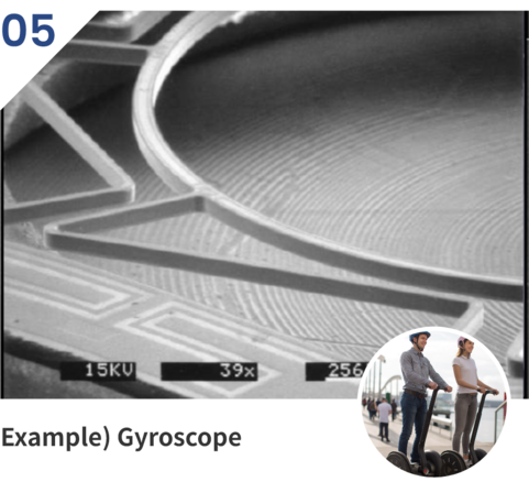
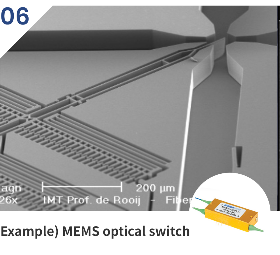
Si DRIE is widely used as a core processing technology in MEMS devices that require microstructures and deep-cut shapes.
You can consult with us from the early stages of development regarding the feasibility of processing and the optimal processing conditions.
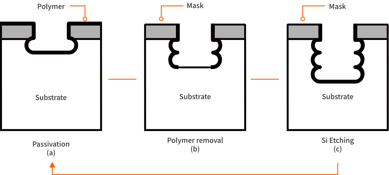
For deep etching of silicon, the Bosch process, developed by Robert Bosch GmbH, is used.
The Bosch process is a silicon etching method that rapidly switches between etching and passivation (sidewall protective film formation) processes.
This switching control allows for deep etching while protecting the sidewalls, enabling high aspect ratio machining and microstructure formation.
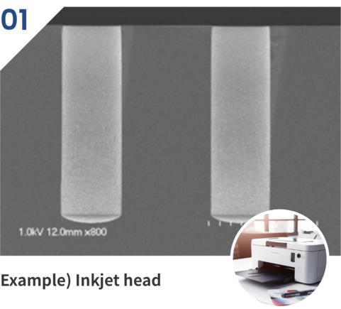
Si Deep Etching (Si DRIE) requires high aspect ratio machining, which allows machining to proceed in the depth direction while maintaining a fine aperture width.
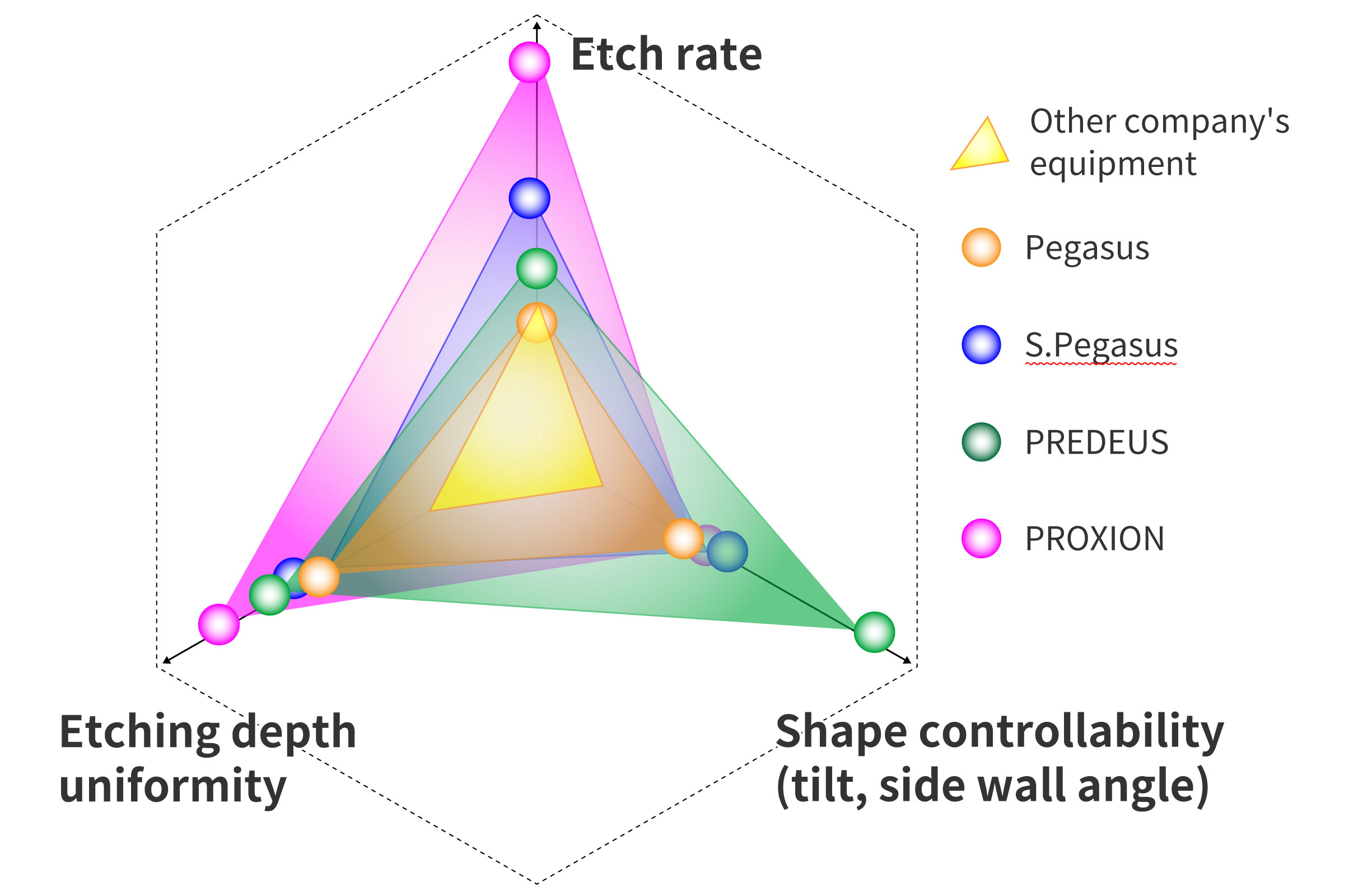
In this type of machining, it is crucial to achieve a high level of balance between multiple factors such as etch rate, shape reproducibility, and sidewall quality.
Through continuous advancements in equipment performance and process control technology, we have improved machining stability and repeatability in high aspect ratio machining.
This enables the formation of complex and highly precise structures required in MEMS silicon processing.
Thanks to improvements in the functionality of our group-developed equipment, the etch rate in Si deep etching has been significantly increased. This enables high-precision MEMS silicon processing while simultaneously shortening processing time and increasing productivity.
In process development, we primarily use Predeus, which offers an excellent balance of etch rate, shape controllability, and depth uniformity, enabling us to stably handle even highly challenging machining conditions.
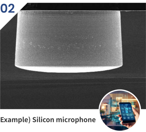
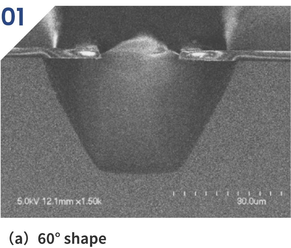
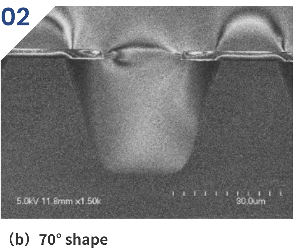
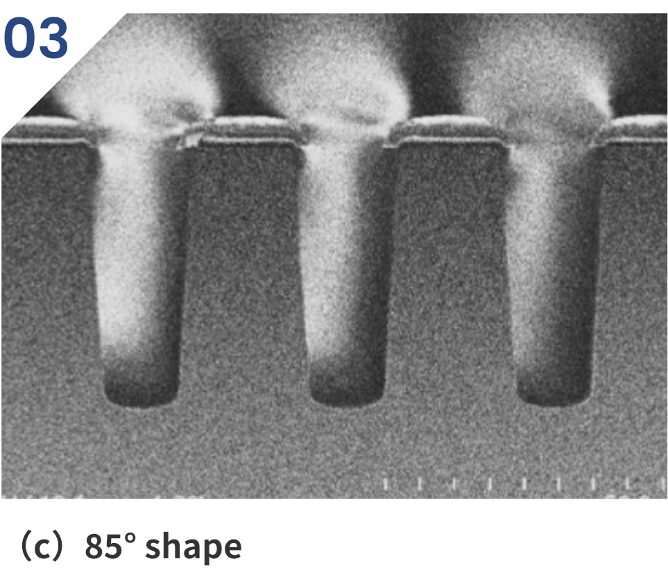
Advances in equipment and process control technology have dramatically improved shape control in Si deep etching.
Even with 200mm wafers, it is possible to stably reproduce a tilt angle of 0.1° or less up to 3mm from the edge.
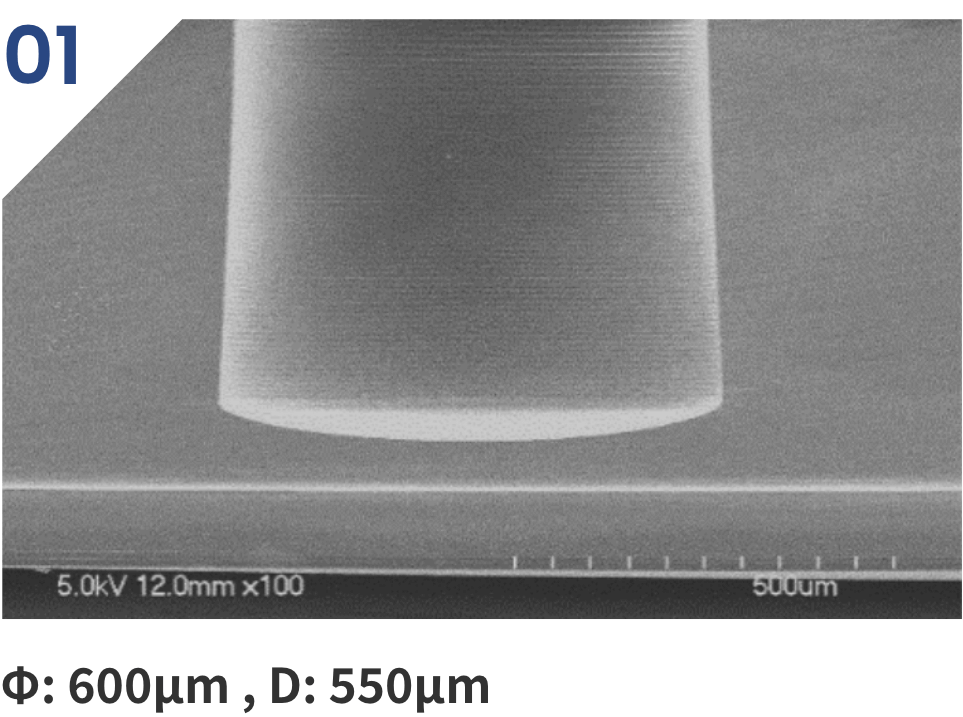
The shape controllability of the in-house developed equipment has been improved, and stable shapes can be reproduced even during deep etching.
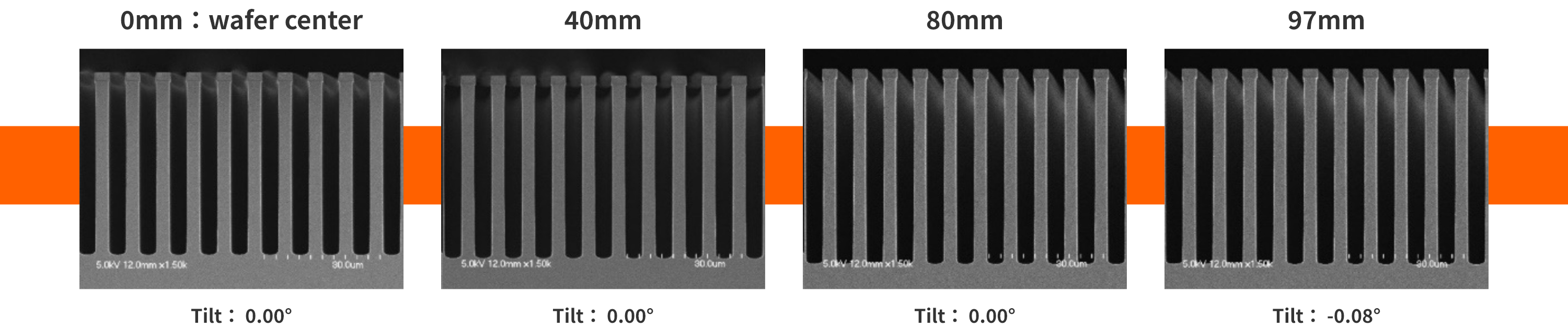
Up to 3mm from the edge of 200mm wafer: Stable control of tilt angles within 0.1° or less
Up to 3mm from the edge of 200mm wafer:
Stable control of tilt angles within 0.1° or less
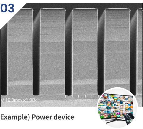
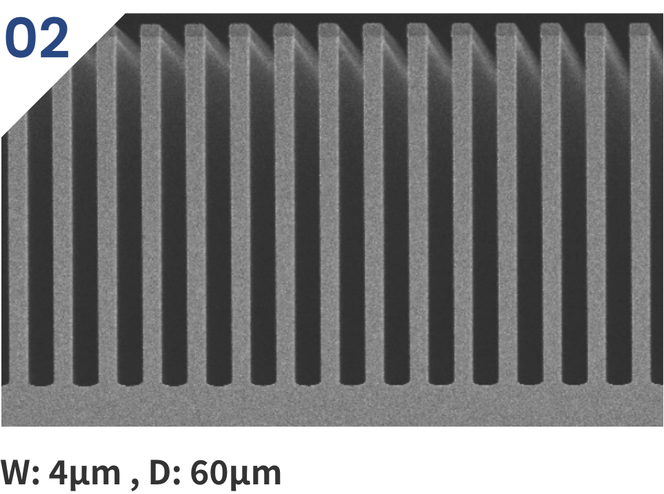
High-speed switching control maintains a sidewall roughness of 16nm even at deep machining depths, achieving high-quality silicon etching with low scallops.
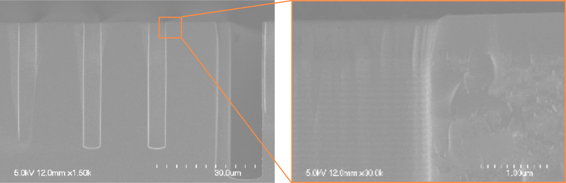
(Sidewall roughness 16 nm, depth 40 μm)
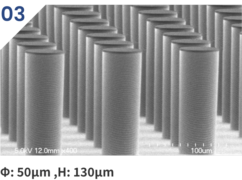
This technology reduces notches at the oxide film interface, a common issue during SOI wafer processing. Even with 30% over-etching under conditions of 3 μm width and 100 μm depth, it enables deep silicon etching without generating side etching (notches) at the oxide film interface.
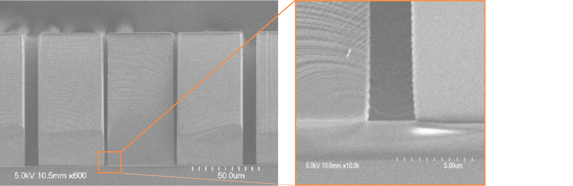
(3 μm width, 100 μm depth, 30% over-etch)
By utilizing parameter ramping technology, we have achieved uniform silicon deep etching with reduced angular deviation and meandering, even in high aspect ratio machining such as 5 μm width and 200 μm depth (aspect ratio 40).
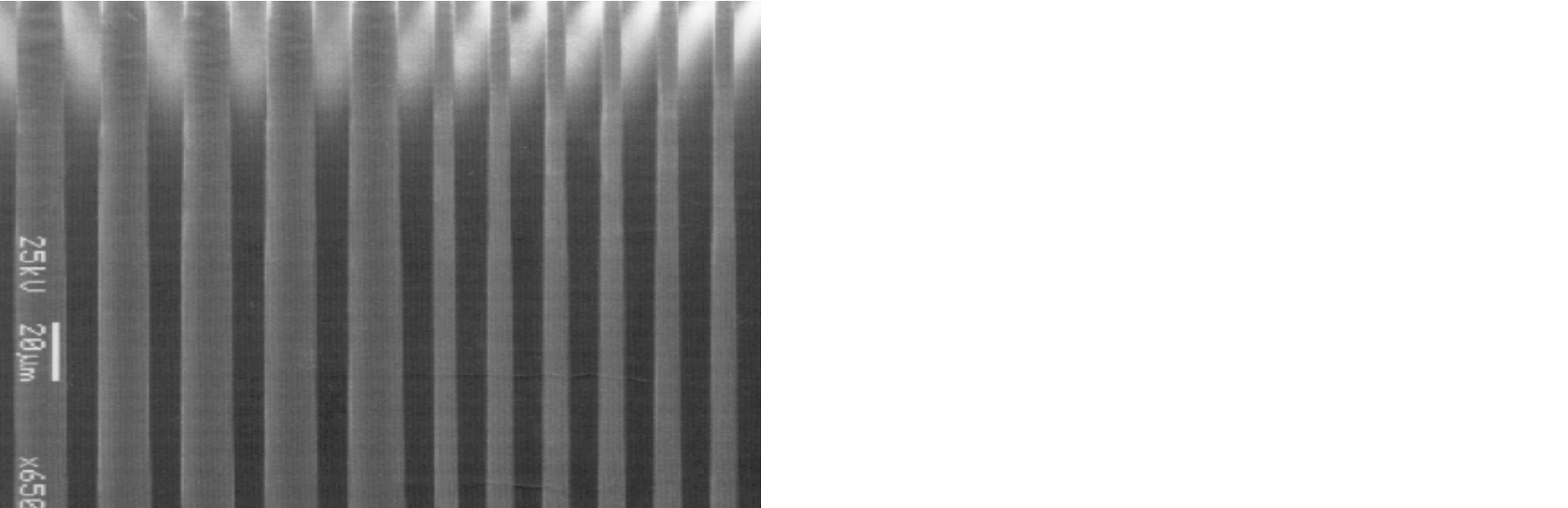
(5 μm width, 200 μm depth, aspect ratio 40)
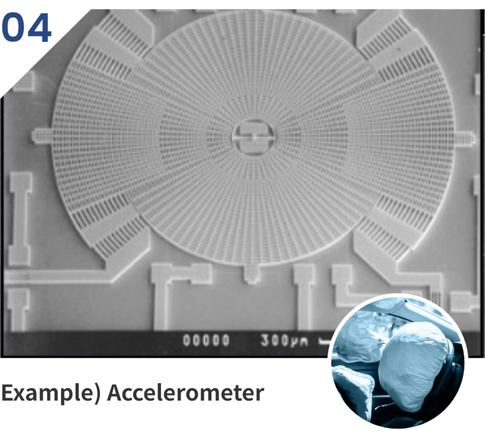
Si DRIE is being applied not only to MEMS silicon processing but also to TSV (Through Silicon Via) formation.
Because it enables high aspect ratio and high-precision silicon deep etching, it can also handle TSV processing, which supports 3D mounting and high-density wiring.
Our company provides comprehensive support, from determining processing conditions during the prototyping stage to process planning and evaluation with a view to mass production, helping to resolve technical challenges in MEMS development and implementation.