pagetop
Contact usContact usContact us

Foundry Development

MEMS Foundry Development

MEMS Foundry Development

Because the microstructure, material properties, and process conditions of MEMS devices interact in a complex way, their performance cannot be guaranteed at the design stage alone.
Translating design intent into actual manufacturing processes, and refining it into a mass-producible form through prototyping and evaluation—this is MEMS foundry development (process development).
Our company provides comprehensive support throughout the entire development phase, from initial consultations at the conceptual stage to prototyping, evaluation, and transition to mass production.
Whether you're a first-time MEMS developer or you have design drawings and are looking for a manufacturing partner, we can provide support tailored to your specific situation.

Regarding MEMS prototype development

MEMS prototype development is a particularly important step in MEMS foundry development.
We then bring the designed device to life through the actual manufacturing process, verifying its performance, structure, and manufacturing conditions one by one.
Many challenges arise only after actually manufacturing, such as process variations in microfabrication, stress and adhesion of thin films, and reproducibility of etched shapes.
In MEMS prototype development, we repeatedly adjust process conditions based on evaluation results to address these challenges and ensure the required performance and reproducibility.
We provide flexible MEMS prototyping support tailored to your specific needs, from initial verification of new devices to validation of existing designs, re-evaluation due to changes in application, and final verification before mass production.
We can discuss options tailored to your development phase and project scale, such as prototyping only after design completion, or prototyping limited to specific processes.

MEMS Foundry Development - Features

MEMS foundry development system based on design collaboration

To accurately reflect design intent in the manufacturing process, our company employs a development system based on close collaboration from the design stage. By designing processes based on structural design and analysis results, we minimize rework during the prototyping phase.
We provide technical consultation from the conceptual stage, and we can support even customers with little experience in MEMS development, from selecting elemental technologies to considering the direction of device structure.

MEMS foundry process for prototyping and small-batch production.

We have established process lines suitable for MEMS prototyping and small-batch production, and we propose the optimal process according to the development phase, from initial prototyping to the manufacturing of evaluation devices.
Because we support phased testing starting with small quantities, it is possible to proceed with development while keeping initial investment low.

Process design with a view to transitioning to a mass production foundry.

We design processes from the prototyping stage with mass production in mind, and proceed with development while considering reproducibility and cost structure during mass production. We organize the conditions and data obtained from prototyping and support a smooth transition to mass production foundry.

MEMS Foundry Development Service Flow

Concept and specification review phase (initial MEMS development review)

We will organize the applications, required performance, and operating environment of MEMS devices to clarify the prerequisites for development.
We will examine the feasibility of your project, taking into account material selection, device structure direction, and anticipated process constraints. We can provide consultation from the elemental technology level, even for research and development applications or new device concepts.

Design and process review (MEMS foundry development)

Based on the preconditions established in the previous phase, process analysis will be conducted in parallel with device design.
We design a process that combines elemental technologies such as PZT piezoelectric thin films and Si deep etching (Si DRIE), and then identify which processes affect performance and yield.

Prototyping, evaluation, and condition optimization (MEMS prototyping)

Based on the results of the design and process studies, we will create a MEMS prototype.
After prototyping, we adjust the conditions while incorporating feedback from the evaluation results to confirm performance, reproducibility, and stability. We can handle everything from evaluation prototypes for research purposes to prototypes for mass production, tailored to each stage.

Consideration of transition to mass production and foundry (pre-mass production development of MEMS)

Based on the prototype results, we will consider whether to transition to a mass production foundry and the process conditions for mass production.
We will help you smoothly scale up your production by proactively identifying potential challenges during mass production.

Our Process Our Process

MEMS Custom Development and Support Scope

MEMS Custom Development

We offer custom development services to optimize device structure and processes to suit your specific application. Without being constrained by existing processes, we consider the underlying technologies and propose process configurations that meet your performance requirements.

MEMS small-lot production available.

We also handle small-lot prototyping and production for evaluation purposes and verification before mass production.
We can provide support tailored to each phase, from small-scale prototyping in the early stages of development to gradual scaling up.

MEMS Prototype Process

We provide each crucial process in MEMS prototyping by leveraging the technological foundations of our company and group companies. For details on specific process technologies, please refer to the following section.

Process technology for MEMS prototyping and foundry

As a MEMS foundry, we provide various process technologies that are crucial for prototyping.

PZT Thin Film Process

We offer our PZT piezoelectric thin-film process, developed within our group and backed by a proven mass production record, as a MEMS foundry service. We can handle prototyping of piezoelectric MEMS devices and ultrasonic MEMS devices, including PZT deposition and etching processes.

Sensor/MEMS Device Application Examples

Sensor/MEMS Device
Application Examples

  • ・Inkjet
  • ・MEMS speaker
  • ・MEMS cooling
  • ・Micro pump
  • ・Ultrasonic sensor
  • ・RF-MEMS
  • ・Pressure sensor
  • ・MEMS mirror
  • ・auto focus
  • ・Energy harvester
Detailed steps of the PZT piezoelectric thin film process. This shows wafer loading, cleaning, thermal oxide film formation, deposition of PZT film (standard 3μm) and upper and lower electrodes, patterning of each layer by dry etching and wet etching, Si patterning by DRIE (deep RIE), and changes in the cross-sectional structure up to substrate thinning (BG).

Si deep etching technology (Si DRIE)

We provide MEMS foundry services for Si Deep Etching (Si DRIE). Having developed the world's first mass-production Bosch process Si DRIE equipment, we possess extensive process recipes and production know-how based on many years of experience in mass-production device manufacturing.
Furthermore, low-scallop processing of 100nm or less allows us to handle devices requiring high-precision structures, such as MEMS actuators and ultrasonic MEMS.

Si DRIE Technology

Low scalloping: 100mm

High aspect

Tapered

Micro-pillar processing

Two-stage processing

Through-hole straight hole processing

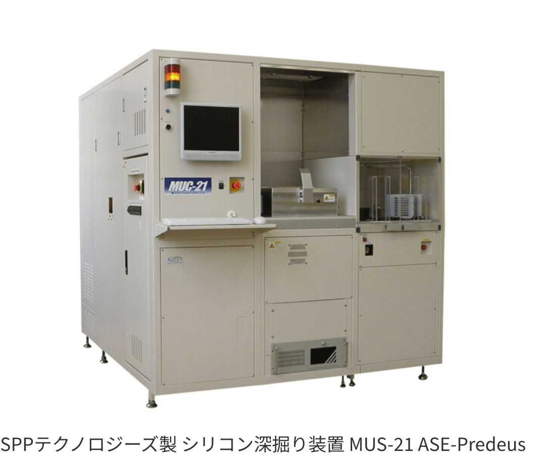
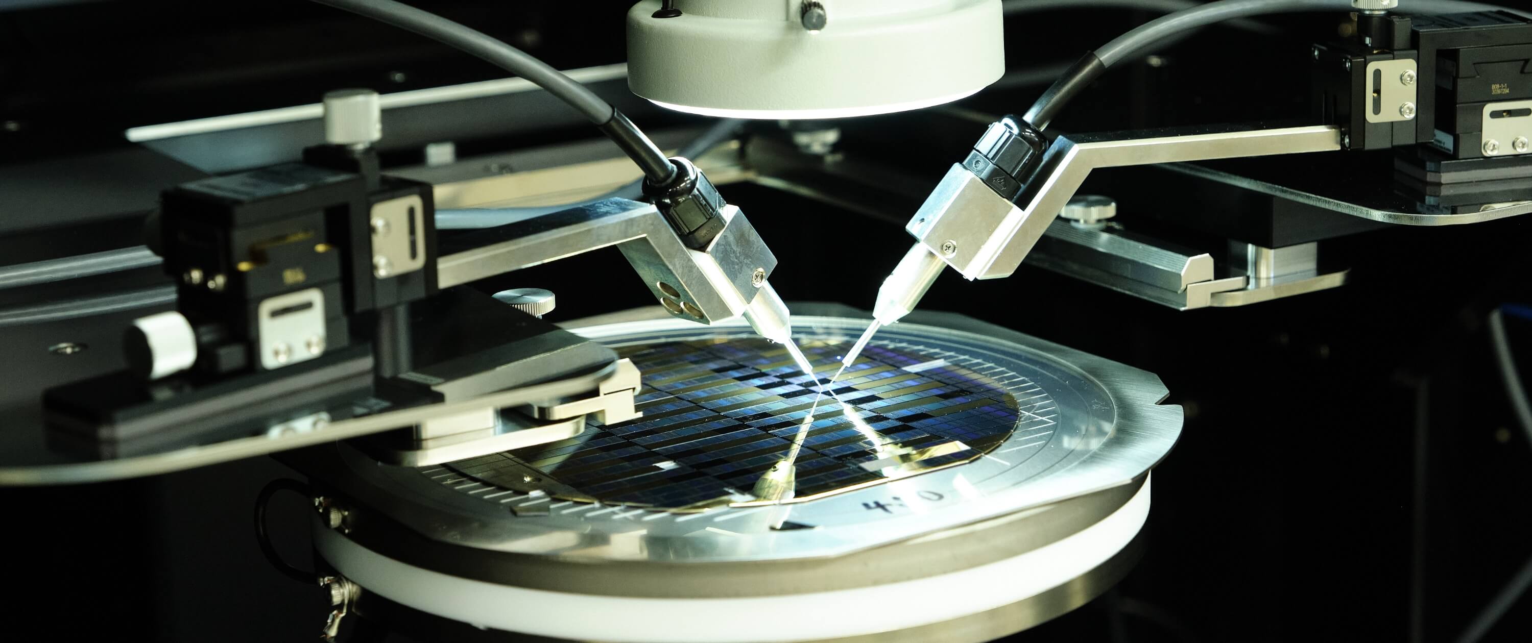
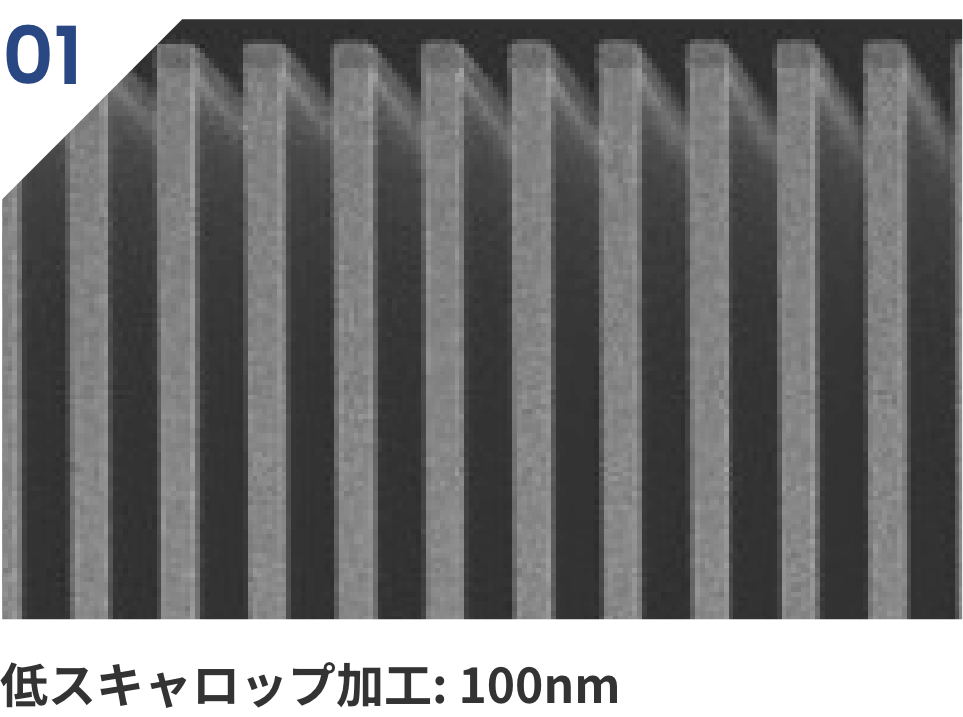
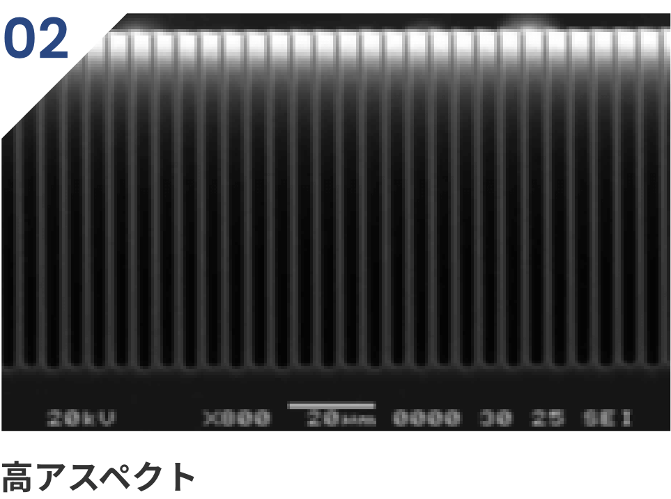
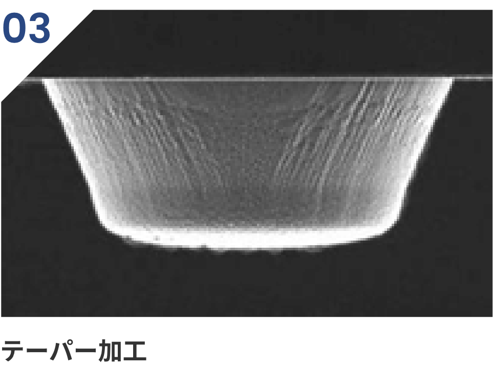
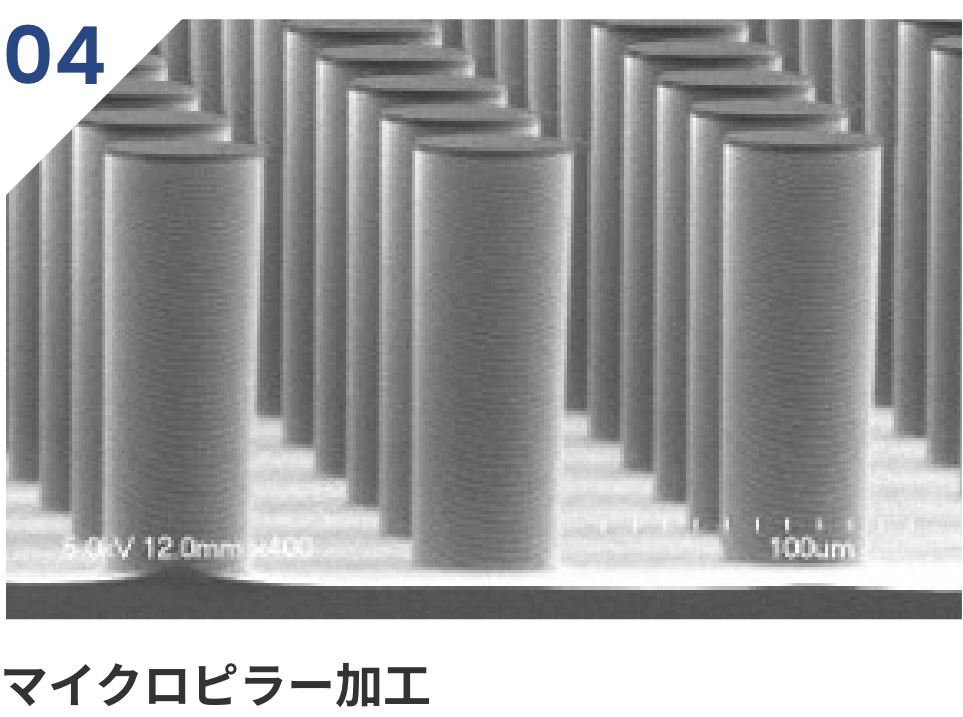
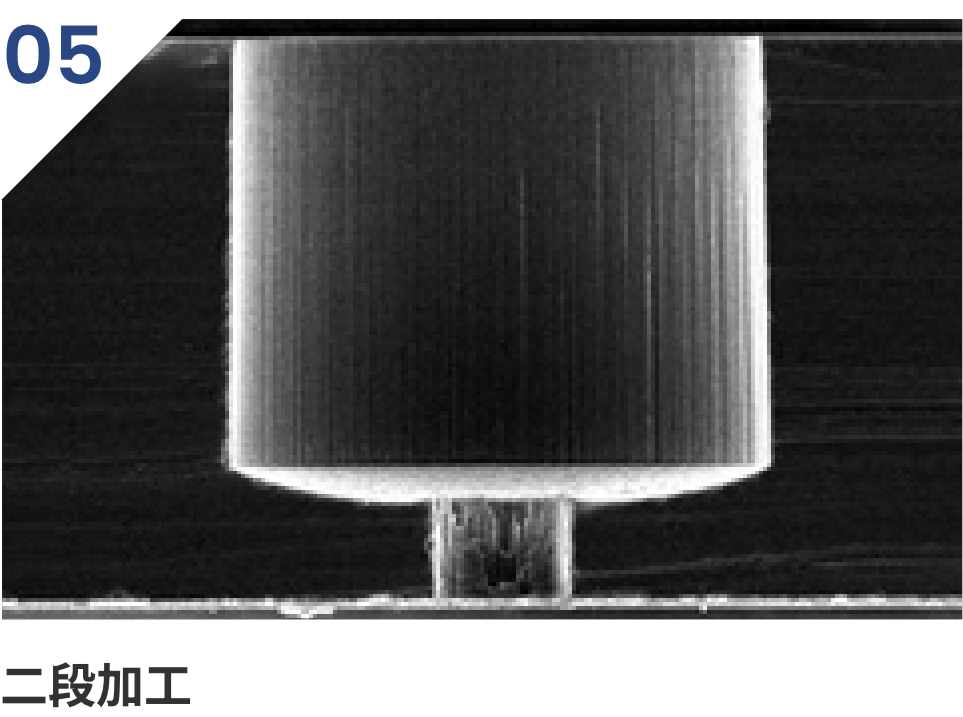
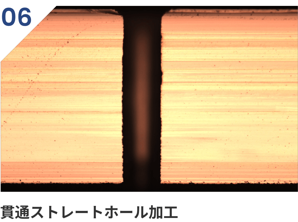
When you work with MEMS Infinity, you gain access to ASE-Predeus, our high-precision Si DRIE system. We've improved the plane uniformity of ASE-Predeus from ±4% to ±3% compared to the conventional ASE-Pegasus. And we've reduced angle control to less than 0.1° at 8 inches. That's an innovation that helps our customers.

SPPテクノロジーズ製 シリコン深掘り装置 MUS-21 ASE-Predeus

Silicon deep etching equipment "MUS-21 ASE-Predeus"
by SPP Technologies

Process menu for MEMS foundries

We offer a variety of process menus tailored to each development phase, including MEMS prototyping, custom development, small-lot production, and mass production preparation, enabling flexible MEMS foundry development according to device specifications.

process Process specifications
etching Si deep etching L/S(min):1.5μm
Hole:φ10μm
Maximum aspect ratio:100
Through-hole processing available
dry etching L/S(min):3μm
Metal film, oxide film, SiC, PZT
sacrificial layer etching L/S(min):1μm
Wet etching Au、AI、Ti、Cr etc
photolithography regist coat Film thickness (max):10μm
Uniformity:5%
Can be spray coated
Exposure
(mirror projection)
L/S(min):1.5μm
Exposure
(contact)
L/S(min):3μm
Double-sided exposure possible
Exposure
(stepper)
L/S(min):1μm
Development
Film deposition
(sputtering)
PZT sputtering *1
Film thickness: 1~5μm *Standard film thickness: 3μm
Relative permittivity: 900 Note1
Piezoelectric constant(d31): 220-240pm/V Note2
The values of Notes 1 and 2 depend on the SSP standard film thickness and film composition.
Metal sputtering *2
Film thickness: 10nm to 5μm
Uniformity: ±10%
Au, Pt, AI, Cr, Ti
Oxide sputtering *3
Film thickness: 2μm or less
Uniformity: ±10%
Film deposition (CVD)
PE-CVD SiO2(TEOS)
※3
Film thickness: 10nm to 5μm
Uniformity: ±5%
PE-CVD SiN
※3
Film thickness: 10nm to 5μm
Uniformity: ±5%
*Stress control possible
Film deposition (ALD)
Atomic Layer Deposition
※4
AI203 and others
Oxidation/annealing thermal oxidation Film thickness: 1μm or less
Uniformity: 10%
Wet/Dry mixture
Anneal
bonding Anodic bonding (can be sealed)
Sealing internal pressure: >0.01Pa
glass processing Blasting L/S(min):15μm
Hole(min):φ50μm
Wet etching L/S(min):10μm
Depth(max):300μm
backend dicing
back grind In-plane distribution: 5μm
Evaluation XRF、EDX
Zygo、SEM
Surface profilometer
Laser microscope etc.

Wafer size: 4 to 8 inches
Please feel free to contact us regarding processes not listed.
*1 The characteristics of the piezoelectric thin film are typical values for our cantilever.
*2 Please feel free to contact us regarding Au, Pt, Al, Ti, Cr and other metal films.
*3 Insulating film is a typical value for various Film deposition methods. Please contact us for more details.
*4 Please feel free to contact us regarding Al2O3 and other protective films.

MEMS prototype equipment and evaluation environment

We possess all the necessary equipment for MEMS prototyping within our company and group, enabling us to provide consistent prototyping support.
Flexible adjustment of equipment conditions allows us to meet a wide range of needs, from research and development applications to mass production preparations.

Coater Developer

Compatible devices and applications

We develop various MEMS devices tailored to specific applications and performance requirements. We provide comprehensive development support, from design considerations based on device structure and operating principles to process design focused on prototyping, evaluation, and mass production.

classification Compatible devices and applications Related technologies and processes
Ultrasonic MEMS pMUT (Piezoelectric MEMS Ultrasonic Transducer) /
MEMS Ultrasonic Sensor
PZT piezoelectric thin film/Si DRIE
Piezoelectric MEMS Piezoelectric sensor / Piezoelectric actuator /
MEMS speaker
PZT piezoelectric thin film
Other MEMS Microfluidics/Micro Pillar/
MEMS cooling and other
Si DRIE

*The above are typical combinations. We can also advise you on selecting technologies and processes according to your application and required performance.

Piezoelectric MEMS

Piezoelectric MEMS are MEMS devices that utilize the piezoelectric effect for driving and detection, and are used in a wide range of applications, including ultrasonic devices, actuators, and acoustic devices.
Our company provides foundry development support for piezoelectric MEMS devices, from initial design considerations to prototyping and evaluation, and we handle process selection and structural design according to the application and required performance.

Furthermore, we possess a PZT piezoelectric thin-film process used in the manufacturing of piezoelectric MEMS devices, enabling us to provide highly reproducible prototypes with a view to mass production. For details on the PZT piezoelectric thin-film process, please refer to our technology page.
*We also offer consultation on piezoelectric materials and process conditions depending on the application and required characteristics.

Piezoelectric MEMS

Ultrasonic MEMS

Ultrasonic MEMS are devices that realize ultrasonic generation and reception functions in a microstructure, and are used in a wide range of fields such as distance measurement, non-destructive testing, and various sensing applications.

Our company provides foundry development support for ultrasonic MEMS, from initial design considerations to prototyping and evaluation. We perform structural design and process selection according to the application and required characteristics. We handle all phases, from conceptual and specification development to mass production transition planning.

pMUT

pMUT (piezoelectric MEMS ultrasonic transducer) is a device that uses piezoelectric thin films to transmit and receive ultrasonic waves, and is attracting attention for applications requiring high sensitivity and miniaturization. By utilizing the PZT piezoelectric thin film process and optimizing the film deposition conditions, structural design, and prototyping conditions, we are able to perform highly reproducible prototyping and evaluation.

MEMS Ultrasonic Sensor

MEMS ultrasonic sensors are sensor devices used to detect the distance to an object and physical changes with high precision.
Our company provides development support, including operational characteristics analysis and sensitivity evaluation during the design phase, and we optimize characteristics according to the application through prototyping and evaluation.

MEMS speaker

MEMS speakers are devices that achieve acoustic output using microstructures, and are characterized by their small size, low power consumption, and high efficiency. In the design and prototyping of MEMS speakers, we provide support for prototype development, including functional verification, by conducting evaluation design and setting conditions based on the manufacturing process.

Microfluidics/Micro Pillar

Microfluidics devices and micropilar structures are typical applications utilizing Si deep etching (Si DRIE) technology. They are used in fields requiring microfluidic channels and high aspect ratio structures, such as biotechnology, medicine, and chemical analysis.
Our company leverages high-precision microfabrication using Si DRIE technology to support the prototyping and evaluation of these devices.

MEMS Cooling

MEMS cooling devices are devices that utilize microstructures to control heat, and their applications are progressing, mainly in heat management.
We provide comprehensive support for MEMS cooling, from process planning and prototype design to evaluation assistance, helping you develop devices tailored to your specific application. Please feel free to contact us.